
The semiconductor manufacturing industry is vast, complex, dynamic, and on the very edge of technological innovation. It is the facilitator of our modern digital world, from smartphones to MRI machines, cookers to space shuttles, everything these days is powered by semiconductor chips, the brain of every circuit board. The demand is high, very high, and to keep up with this, companies, such as Samsung, TSMC, Onsemi and Texas Instruments, produce over 1 trillion semiconductor chips each year, that’s enough for every person on the planet to receive 150 chips each, every 365 days! With such high demand and vast quantities produced, there is a strict requirement for absolute precision and efficiency from the manufacturing process, and this procedure isn’t simple in the slightest.
Reducing Waste & Boosting Efficiency: How the Semiconductor Industry is Embracing Repair to Drive the Future of Sustainability
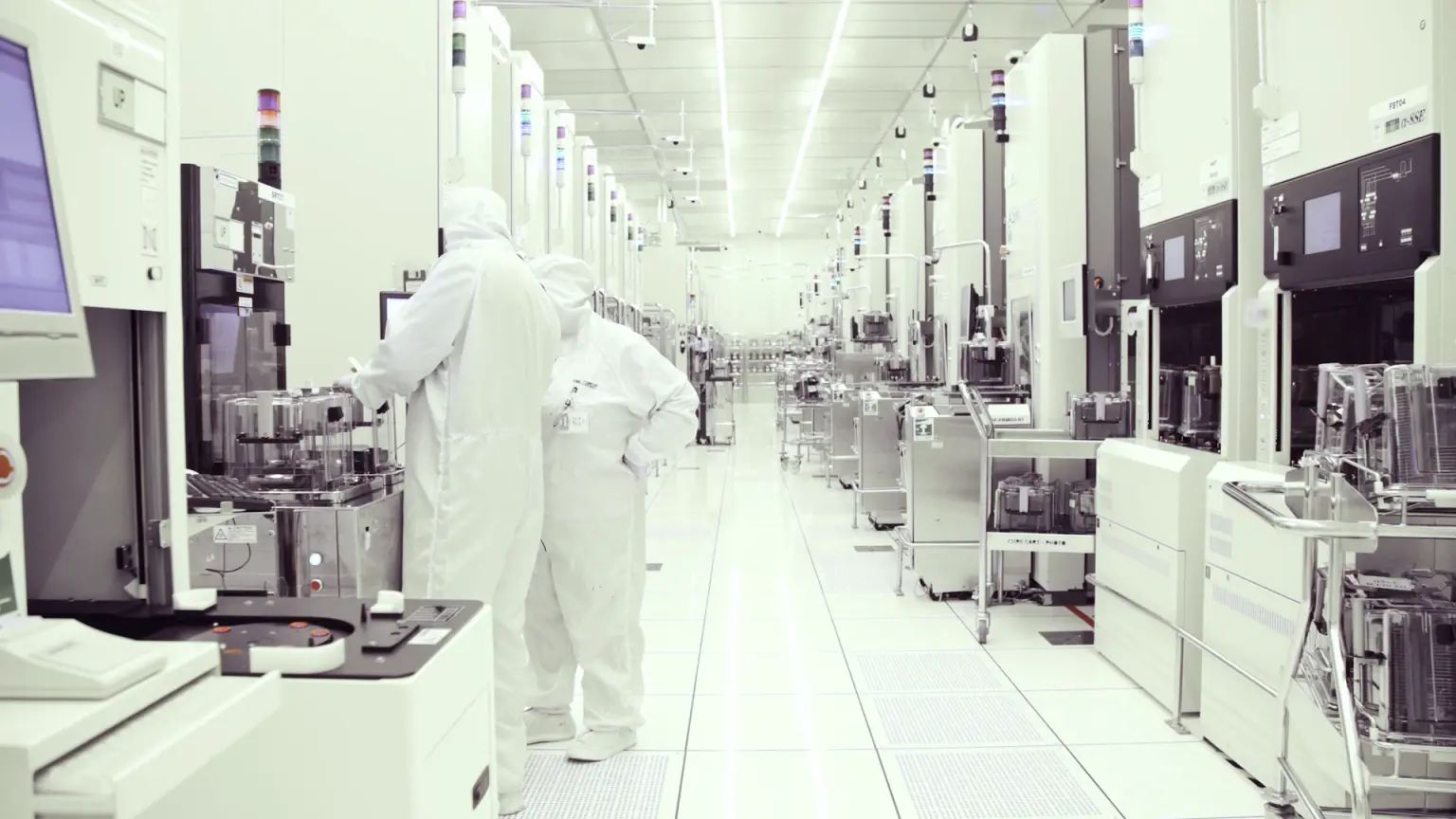
A chip is made up of a silicon base containing billions of transistors, electronic switches, and a vast network of nanowires within an insulator substrate. To manufacture these, a contaminant-free environment is essential as even a single dust particle can ruin an entire batch. Production takes place in factory-sized clean rooms and follows a multi-step process that begins with a polished silicon wafer sliced from a pure silicon ingot. Wafers are moved from machine to machine for each step of the process via an automated overhead transport system, to prevent contamination. In the first stage, a layer of non-conducting silicon dioxide is applied as an insulator, followed by a light-sensitive photoresist solution. UV light is passed through a stencil and miniaturised by lenses, which hardens the exposed photoresist, allowing the unexposed area to be washed away leaving a microscopic mask of the stencil, in a process called photolithography. The underlying exposed silicon dioxide is then etched away by hot gases, the mask is removed and a metal layer, usually copper or aluminium, is applied to fill the gaps. This is planned back to the SO2 level leaving nano tracks of metal. This process is repeated 80 times over 12 weeks for an 80-layer chip. Finally, the wafer is laser-cut into individual chips, which are tested using ATE machines, to determine their computational capabilities and application.
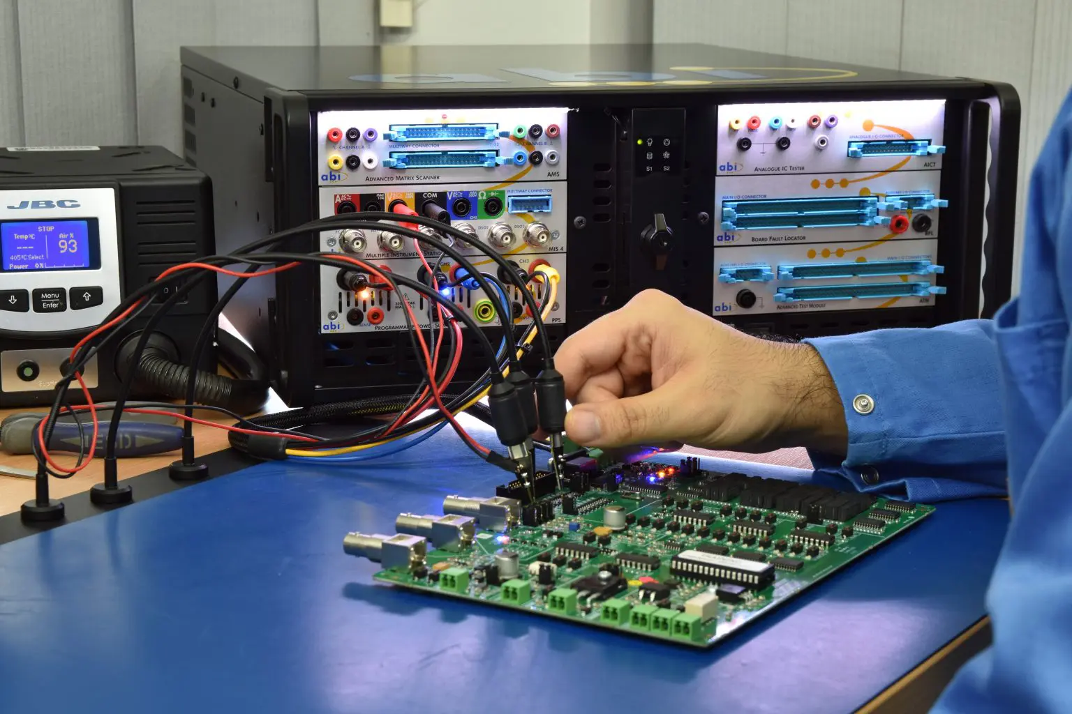
Each of these steps and sub-steps is operated by multiple machines, costing anywhere from a few million to $170 million each! With these machines carrying such a high cost and the high-pressure demand of chip production, semiconductor fabs can’t afford any errors or breakdowns within the production line. Any machine downtime means the entire systematic, rotational operation grinds to a halt, costing millions in lost revenue, and restarting production can be very challenging. However, inevitably things do go wrong with electronics and circuit boards, so these fabs must have quick response processes in place to reduce the downtime. While it might seem enticing to dispose and replace parts in a wasteful cycle, the cost of having a vast inventory of spares can be huge. So, if constant replacement isn’t the answer, what is?
Recently, within the semiconductor sector, there has been a large growing movement advocating for repair, shifting industry attitudes away from replacing. This pivot to more sustainable and obsolescence-mitigating practices comes as concerns continue to grow over E-waste generation. As more and more electronics are manufactured every day, greater amounts will be disposed of in favour of new ones, with 85% still ending up in landfill, polluting our environment. With fabs and equipment manufacturers pushing for greater environmental efforts, it has become clear that E-waste production is closely linked to future sustainability. But the benefits of electronic repair don’t stop there, especially for the semiconductor space. These companies adopting the #RepairMindset, have experienced significantly reduced downtime without the need of a vast and costly inventory of spares. The boards removed can have their faults diagnosed, repaired, tested and put into storage for later use or integrated straight back into the equipment. This can save huge amounts of money on unnecessary spares, especially when a single ATE card replacement can cost upwards of $100,000, and the evidence is apparent!
A US-based multinational semiconductor manufacturer sent us this quote last month:
“Since January, I have fixed 105 high-value circuit boards and saved the company over $525,000. They’ve even given me a nice pay rise!”
That is half a million dollars in 6 months saved just by repairing instead of replacing some of their faulty circuit boards!
The embrace of our Repair Don’t Waste mindset allows these companies to reduce their environmental footprint and simultaneously improve their bottom line. By investing in repair processes and training technicians to diagnose and fix faulty boards, semiconductor manufacturers can avoid the enormous costs associated with machine downtime, obsolescence and unnecessary replacement of high-value components. Repairing circuit boards has shown to save millions proving that this method can be both economically and environmentally advantageous. This repair-driven approach, also aligns with global sustainability goals, contributing to the circular economy, and as governments and industries alike push for greener practices, semiconductor manufacturers are increasingly expected to lead by example. Repairing, reusing, and reducing waste are key pillars of this movement, helping companies maintain a competitive edge in a rapidly evolving market.
The semiconductor manufacturing industry stands at the crossroads of innovation and sustainability. With the world’s reliance on semiconductor technology growing each day, the need for precision, efficiency, and environmental responsibility has never been greater. The pivot to repair over replacement marks a significant step toward reducing E-waste, lowering costs, and ensuring that the industry continues to power the digital world responsibly. By embracing the repair mindset, semiconductor manufacturers are not only ensuring their own future but also contributing to the broader goal of global sustainability.